

Is currently a Feature Integration Engineer – Vision Systems at General Motors (GM). Sai is the Subject Matter Expert for GM’s Image Quality. Being a collaborative, cross-functional Global Autonomous Driving Center’s key team player, he is very much focused towards the ultimate customer satisfaction by developing new methods, simulation models and test equipment for vehicle level testing of Image Quality at GM. Sai’s interests include Tool Scripting, Active Safety Viewing Systems, Computer Vision, Artificial Intelligence, Object Recognition, Pattern Recognition, Cyber-Security, and Simulation. He was an Active Safety Performance Engineer – Vision Systems (2015 to 2018) at GM. His innovative approach led to outlining and execution of GM’s Image Quality vehicle level testing strategy. Sai is the technical lead on Image Quality for multiple industry-first vision systems related features. He has 10+ US patents in viewing systems, pattern recognition, object recognition. Sai got his Masters in Electrical Engineering from Wayne State University, a Bachelors in Electronics and Communication Engineering from Swami Vivekananda Institute of Technology, a Diploma in Computer Applications and a Diploma in Multimedia.


Scott is both co-founder and co-dreamer at Sense. He has 30 years of commercial and innovative product experience in III-V compound semiconductors and optics. Before Sense, Scott served as Executive Vice President of manufacturing and technology development at Semprius Corp, Vice President of Engineering at Santur Corporation, Vice President of Technology at Optovia, and Vice President of Operations at CoreTek, a successful tunable laser start-up acquired by Nortel. Scott started his career at AT&T Bell Laboratories, where he helped to develop and manufacture GaAs semiconductor lasers for the world’s first commercial fiber optic communication systems.


Dr. Leilei Shinohara joined RoboSbense in January, 2019. He is responsible for the Automotive LiDAR development. He has more than ten years experiences with LiDAR development crossing the phase of advanced development and research, standardizing, customer specific development, and the transaction from R&D towards to massive production.
From 2015 to 2018, he was the Technical Lead for Asia OEMs at Valeo, and was responsible for automotive LiDAR, automotive active safety products, and sensor fusion. He was responsible for a development team with systems, software, hardware, mechanics, testing/validation, and functional safety for the first automotive grade LiDAR product “Valeo Scala”.
In 2008, Dr. Shinohara began his PhD studies at Karlsruhe Institute of Technology in Germany, and received his PhD degree in Electrical and Electronics Engineering in 2014. During six years of PhD studies, Shinohara focused on LiDAR systems and was involved in several projects, including optical sensor system design, optical quality measurement, Doppler LiDAR, and 3D MEMS micro-mirror LiDAR for autonomous driving.


Based in Canada, Patrice heads Immervision’s engineering as well as, contributes to IP growth and the adoption of Immervision’s wide angle panomorph technology by global corporations. He has overseen the integration of wide-angle imaging technology in numerous consumer electronics, surveillance, automotive, aerospace, medical and broadcast products. Recently, he has led the miniaturization of the panomorph wide angle technology for smartphones, tablets, wearables and IoT devices.
Back in 2000 in France, after completing his Master’s degree in image processing and computer graphics, Patrice joined the INRIA and contributed to their research in robotic surgery simulation field. In parallel, he co-founded Immervision, a company dedicated to wide angle optics and imaging technology. With his conviction that wide angle technology could be applied everywhere, he contributed to the development of wide angle panomorph optical and imaging technology.
Beyond technology, Patrice believes that innovation is propelled by human beings, partnerships and alliances - he has collaborated with a large ecosystem of partners in the optics industry like Fujifilm, CBC Computar, Tamron and Kolen, and in the silicon industry like Marvel, Intel, Qualcomm, Sony, Samsung, HiSilicon, NXP and OmniVision. In addition, Patrice is an avid surfer, international traveler and always seeks to make new connections.


Avi Bakal, Co-Founder & CEO of TriEye has achieved a mass-scale technological breakthrough in record time, creating a giant leap in ADAS & AV safety, reliability, and functionality. Avi is an experienced multidisciplinary Physicist and Electrical-Engineer. He has a BSc in Computer Science & Electrical-Engineering and an MSc in Applied Physics specializing in optics and lasers. Avi served as a combat commander in a special Air-Force unit. Earlier this year, he was named as CEO of the Year by ISE.


Barmak brings over 25 years in mixed-signal integrated circuit design, semiconductor device physics and device micro-fabrication with specialization in active pixel sensors (APS), infrared focal plane array technology and high-speed communication. Previous to founding Forza Silicon, Barmak was with Photobit Corporation and NASA JPL’s Advanced Imager Technology Group. Barmak holds 17 patents in image sensor design and has contributed to over 20 articles in imaging and high-speed data communication. He received his BSEE and MSEE degrees, as well as his Ph.D. in Electrical Engineering, from UC San Diego.
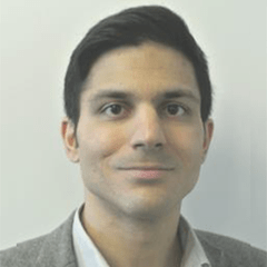
Bahman Hadji has over ten years of experience working with sensing devices for medical, consumer, and automotive applications. In his current role with the SensL Division of ON Semiconductor’s Intelligent Sensing Group, he is focused on bringing to market high-performance sensors used in LiDAR systems and enabling the LiDAR technology ecosystem to leverage ON’s product portfolio. Prior to joining ON Semiconductor in 2017, he held product engineering and product marketing management roles at Aptina Imaging and OmniVision Technologies. Bahman obtained his Bachelor of Applied Science in Computer Engineering and Master of Applied Science in Electrical and Computer Engineering degrees both from the University of Waterloo in Canada.


Jon Barad, VP of Business Development at Velodyne Lidar, is currently leading the Company’s efforts in engaging and developing strong partnerships with companies in emerging autonomous markets, including robotics, drones, trucking, smart cities, security, and more.
Jon has previously held positions within the executive leadership teams at NVIDIA, EDGE3 Technologies (a vision analytics company), and Recommind (acquired by OpenText).
His career started in Venture Capital at ITU Ventures, leading him to co-found OrganicID, which was subsequently acquired by Weyerhaeuser in 2006 for its 3D printing technology.
Jon holds a BS in Systems Engineering from the University of Pennsylvania and an MBA from Harvard Business School. He is a kidney donor, and lives in Mill Valley, California with his wife and two young boys.


Beat De Coi is founder and CEO of Swiss based ES-PROS Photonics corporation. He and his team devel-oped a backside illumination imager technology, which allows to build sensitive CCD charge manipula-tion elements within CMOS chip devices. With this technology, high speed imaging, time-of-flight dis-tance detection as well as wide band spectral sensing devices are available on the market. Beat De Coi is elected member of the Swiss Academy of Technical Sciences SATW.
ESPROS Photonics is a world-class foundry, product, and technology solution provider for optoelectronics manufacturers, imager designers, and researchers. The privately owned company with more than 70 employees working in the Swiss headquarters was founded in 2006 by Beat De Coi.
www.espros.com